
Parylene is often applied to substrates or materials where there is no room for any voids in the protective coating. These materials are likely to be placed in harmful chemicals, a moisture packed environment, or even the human body. These are often mission critical devices which can not allow any environmental factors to alter their performance. Whenever these devices need this stringent level of protection from the elements, parylene is the only logical choice.
Uniformity Explained
Parylene is often applied to substrates or materials where there is no room for any voids in the protective coating. These materials are likely to be placed in harmful chemicals, a moisture packed environment, or even the human body. These are often mission critical devices which can not allow any environmental factors to alter their performance. Whenever these devices need this stringent level of protection from the elements, parylene is the only logical choice.
Parylene coatings are completely conformal, have a uniform thickness and are pinhole free. This is achieved by a unique vapor deposition polymerization process in which the coating is formed from a gaseous monomer without an intermediate liquid stage. As a result, component configurations with sharp edges, points, flat surfaces, crevices or exposed internal surfaces are coated uniformly without voids, as shown below:

Here the orange layer is parylene, with completely uniform coverage of the substrate (illustrated in green), leads (in grey), and component (in black). This all encompassing coverage is one of parylene’s greatest competitive advantages against other liquid conformal coatings. Let’s look at what a liquid coating’s coverage may look like:

Despite the poor editing, it is easy to see that on the sharp edges the coating is substantially thinner than at other areas. There is also pooling on the sides where the leads meet the connector. Factors like this are inherent with liquid coatings, simply because they are a liquid.
Parylene Chemistry and Production Requirements
ParyIene's unique vapor-phase polymerization differs considerably from the application processes of other coating materials. More complex, the technique deposits the substance directly onto the material being coated in a manner that penetrates deeper into the substrate surface. Implemented in a specialized vacuum chamber, parylene's application process does away with the intermediate liquid deposition procedure common to competing coatings.
Chemically, the various parylenes' main-chain phenyl group generates reliable molecule-to-molecule interaction, while possessing high levels of in-plane electronic polarization capabilities. Because these molecular layers are room temperature and chemical vapor deposited (CVD),
Thus, parylene's molecular layers are particularly valuable for microelectomechnical systems (MEMS) and nanotechnology driven applications, which emphasize simplifying component manufacturability.
Unfortunately, compared to other coating options, more time is generally needed to assure parylene's superior conformal coating of targeted substrates, a consideration that needs to be an integral component of manufacturing strategies. For instance, the fact that coating thicknesses from 0.10 micron to 76 microns can be applied in a single operation enhances the quality of completion of manufacturing processes. In general, however, slower production time leads to:
Parylene Deposition Rates and Process Duration
Parylene's application process is rather different and, in consequence, slower and more expensive than the traditional wet chemistry coating methods used for acrylic, silicone and other substances. The parylene process is multifaceted, involving several steps. Unlike many competing application processes, parylene deposition is not line-of-sight. Rather, the gaseous monomer uniformly encapsulates all sides of the object being coated simultaneously.
While CVD generates the truly conformal nature of parylene coating, it can be considerably slower to implement. In addition, appropriate cleaning, activation and masking precede CVD coating in the deposition chamber. Deposition rates for parylene conformal coating vary, often significantly, according to:
Conclusion
Biologically and chemically inert, parylene responds well to the CVD process. Not requiring the liquid phase application standard from most competing coating materials, parylene provides an authentically conformal covering. The excellent barrier strength is characterized by a completely pinhole-free and uniform thickness. Coating application is controllable at thicknesses > 0.5µ, while effectively penetrating product spaces as narrow 0.01mm, making parylene highly relevant to MEMS/nano uses.
Confirmation of these standards is as important to Diamond as it is to our valued customers, and contributes to production time. However, the attention paid to quality throughout all stages of the parylene coating process engenders enhanced delivery of client expectations. It simultaneously generates substrate coatings guaranteed to maintain component protection and performance for the duration of its expected operational life.
Points to Consider
The polymer parylene (XY) provides exemplary, ultra-thin conformal coating for printed circuit boards (PCBs), solar cells, light emitting diodes (LEDs), medical implants, aeronautical/military equipment and numerous other products, with uniform, insulative protection in the nanometer (nm.) range.
One of XY’s basic advantages is its reliable coating uniformity, exceeding that of liquid materials like acrylic, epoxy, silicone and urethane. Rather than brushing dipping or spraying pre-synthesized layers onto substrates, parylene’s chemical vapor deposition (CVD) application method synthesizes the conformal film in process. Parylene’s deposition system consists of a series of vacuum chambers that sequentially produce parylene vapor, pyrolyze it, deposit it as a polymer, and then capture its effluent.
Parylene is unique in being created directly on the surface at room temperature, and is widely regarded as the ultimate conformal coating for protection of devices, components and surfaces in electronics, instrumentation, aerospace, medical and engineering industries. In process, gaseous XY seeps deep into the substrate surface as well as building coating protection along its exterior, generating a double layer of conformal protection. Coating layers are far thinner than those provided by liquid materials, enhancing parylene’s functional versatility.
Nevertheless, XY’s layer uniformity is not always precise. This is far more often the result of deviation or non-conformity along the substrate surface than because of defects with the parylene material or the CVD process. This is not to suggest that:
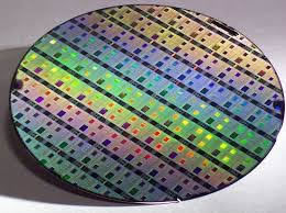
Problems do occur with both material and process, especially if the wrong XY type – C, N, F D, etc. -- is selected for a coating assignment when another parylene variety will provide better coverage. However, deviations in parylene uniformity are far more frequently generated by variations in substrate topography. In these cases, parylene consistently provides an effective conformal coat. But there are instances where substrate features interfere with the overall and precise uniformity of the deposited XY film. Surfaces of semiconductor wafers can cause this problem to develop.
Moreover, the surface geography of semiconductor and sensor wafers is not a defect, but typical of their structure. According to international software engineering standard ISO/IEC 25010, it does not qualify as defective nonconformity or nonfulfillment of a quality requirement for intended usage. Indeed, standard wafer topography tends to be varied and is essential to its quality performance, particularly for wafers containing multiple chips. The parylene deposition process is the most efficient for accommodating these surfaces, since its vaporous consistency surrounds all areas on the wafer’s surface, penetrating within as well as forming a protective outer film layer.
Evidence repeatedly demonstrates CVD’s extreme utility as a method of thin film deposition on wafer and other similarly irregular substrates. XY’s prominence as a conformal coating rests largely on its ability to effectively cover component configurations with sharp edges, points, flat surfaces, crevices or exposed internal surfaces; normally, these are coated uniformly without voids. There are exceptions. While coating wafers will be complete in terms of coverage, a tendency toward minimal non-uniformity can develop.
Because of the exceptionally thin coating layers provided by parylene, non-uniformity will similarly be slight. A recent study showed that, through nine samples, average deviation in coating uniformity did not exceed –1.0 nm. or +1.5 nm., across the entire production run. Coating thicknesses also varied slightly according to which shelf in the deposition chamber the wafer was situated during CVD. The highest of the three deposition shelves averaged a coating thickness of 274.35 nm., the thinnest layer of the batch, perhaps because there were no obstacles above the sample situated at this level obstructing its vaporous movement. Layers were progressively thicker on the lower shelves; the middle shelf averaged 295.12 nm., the bottom and most spatially-confined shelf, 308.52 nm.; there was less room for the vaporous XY to circulate there, causing it to settle on the wafer’s surface.
Thin conformal films generated by parylene CVD tend typically to be exceptionally uniform, even in the nm. range. However, research evidence shows that differences in both
For wafers, a deposition footprint can emerge, wherein coating uniformity in the wafer’s center deviated to the extent that film thicknesses were slightly greater at substrate boundaries and wafer edges/rims. Development of shadowing --
Can occur if the CVD process is not appropriately monitored. CVD processing of semiconductor wafers offer a rare instance where non-uniform parylene deposition occurs, although at an insufficient level to effect unit protection or function.