
Parylene (XY) conformal coatings are known and recommended because of their many beneficial performance characteristics. They provide uniform, pinhole-free protective films with excellent barrier/dielectric/insulative properties, able to conform to virtually any substrate configuration.
A Comparision
Parylene (XY) conformal coatings are known and recommended because of their many beneficial performance characteristics. They provide uniform, pinhole-free protective films with excellent barrier/dielectric/insulative properties, able to conform to virtually any substrate configuration. One property in particular – micron-thin coating layers – distinguishes XY from liquid coating materials such as acrylic (AR), epoxy (ER), silicone (SR) and urethane (UR), which need to be applied at least twice as thick in most cases and frequently more, limiting their range of uses. Parylene typically is applied at 0.1 to 50 microns (0.004 -2 mils), while the thicknesses of liquid coatings generally range from 25 to 250 microns (1-10 mils). Compared to liquid processes, gravity and surface tension generate negligible impact with parylene, eliminating film bridging, pinholes, puddling, run-off, sagging or thin-out during application. XY’s coefficient of friction coefficient can be as low as 0.25 to 0.30.
More likely to be applied in exceptionally thin layers, parylene protects the items it coats. However, being thin and being clear can also be a disadvantage. For instance, SR’s thicker coating level adds an additional layer of cushioning and shock protection to the printed circuit board (PCB) or assembly it covers. Parylene requires several layers of coating to provide even similar impact resistance. In general, thinner is better for XY but, as with all uses for all conformal coatings, much depends upon the specific coating project and its functional requirements, post-application, after operation commences.
This condition can be illustrated for parylene by two cases, concerning XY’s insulation resistance (IR) and breakdown voltage (BV) performance:
Regardless of type, parylenes display:
This condition is opposite than that for parylene IR, where thicker layers offer greater protection.
However, despite certain operational cases where thicker parylene coatings offer better performance, thinner XY coating layers represent one of the materials greatest functional advantages. Thinner coatings respond optimally to proliferating development of microelectromechanical systems (MEMS) and nanotechnology (NT) applications, which can have operating components in the micrometer (0.001 mm)/nanometer (a billionth [10-9] of a meter) functional range. MEMS/NT require the same protections from contaminants as larger components; of conventional coatings, only XY can provide coating functional at these minute levels. Parylene’s use for biocompatible implants is also best-served by thinner coating levels, which work effectively internally, where operating clearance can be too small for effective liquid coating.
Parylene also offers excellent dry-film lubricity for implant and surgical instruments, providing wear and abrasion resistance. XY’s low surface energy and hydrophobic properties generate reliable solutions to the friction/stiction problems affecting biomedical and MEMS/NT applications. In most cases, thinner XY coats are preferable to thicker.
Points to Consider
Each conformal coating material exhibits a range of unique performance properties that determine its product uses. Relevant factors include the required coating-thickness necessary to assure reliable performance. Like other coating types, parylene (XY) layer thickness is largely a function of several factors: (1) substrate material, (2) the kind of assembly being covered, and (3) its operational purpose. Chemically inert parylene is effective at far-thinner application thickness than liquid-applied materials for coating printed circuit boards (PCBs) and related electro assemblies:
XY’s chemical vapor deposition (CVD) process is a primary reason for its thickness advantage compared to wet substances. Consistently pinhole-free conformal films that penetrate even the smallest surface crevices on a molecule-by-molecule basis provide XY a unique advantage in this regard. Gaseous XY seeps deep into substrate surfaces, effectively adding a layer of protection beneath the assembly surface, as well as above, on the component’s exterior. With operating thicknesses in the 0.1 micron range, XY is exceptionally adaptable for microelectromechanical systems (MEMS)/nano-tech components, expanding their applications far beyond those of liquid coatings. To illustrate the scale involved,
CVD parylene polymer film thicknesses are controllable to less than a single micron (1 μm.), or 1,000 nms., supporting XY’s adaptation to functional systems operating at the molecular scale.
Parylene coatings are flexible, uniform at controllable, pinhole-free thickness. XY-coating remains adherent and intact, preserving dielectric/insulation properties, at thicknesses greater than 0.5µm., completely penetrating spaces narrow as 0.01mm. Parylene resists chemicals, corrosives, moisture and solvents, with minimal thermal expansion, covering virtually any board topography, while ensuring PCB/assembly function/performance through most operating conditions.
However, each parylene type exhibits a collection of unique performance properties that determine appropriate applied thickness and subsequent product uses. As with other conformal materials, coating thickness is determined by assignment specifics – substrate material, assembly type, operational requirements.
Coating thicknesses must meet quality specifications. Parylene’s exceptionally thin coatings distinguish it from liquid coating materials, but also require a similarly specific connection between the coating’s final thickness and the functional requirements of the component during operation. As with all conformal coatings, applying XY films too thin eventually renders the PCB vulnerable to a wide range of environmental/performance threats, negating the coating’s protective function. Applied too thick, conformal coatings interfere with an assembly’s operation, particularly for those with moving parts.
Accurately deposited in a single coating-run between 0.5 microns through 50+ microns (2 mm.), typical XY thickness standards are in the 15 micron range, according to IPC CC 830 and MIL-I-46058C guidelines. Here again, coating purpose largely determines its ultimate thickness:
Operationally, the coating process runs until all the dimer is vaporized and deposited. Final XY coating thickness is further determined by the quantity of parylene dimer vaporized relative to the assignment’s overall load surface area. Thus, dimer quantity needs to be carefully calculated and controlled, based on the surface area of the load in the deposition chamber. Because the association between dimer quantity and surface area is so critical to the success of each coating assignment, the most consistent coating thicknesses are achieved with similar size production lots. Odd lots, or those of divergent sizes, require additional focus to project specifics to ensure appropriate coating thickness.
A Comparison
Of the five most commonly used conformal coatings, four – acrylic (AR), epoxy (ER), silicone (SR) and urethane (UR) – are classified as wet materials, meaning they are applied to substrates by three basic types of liquid-based technology:
A fifth conformal coating material, parylene (XY), is not applied as a wet substance. Rather, a unique chemical vapor deposition (CVD) method transforms solid, powdered parylene dimer to a gas which permeates substrate surfaces, providing an under-, as well as an over-layer, of conformal protection. The process allows uniform conformal film application to virtually any surface topography and material, including ceramics, ferrite, glass, metal, paper, plastics, resin, and silicone. These capabilities far exceed those of liquid coatings.
Coating application methods substantially impact the thickness of film deposited on substrates.
Coating Materials and Film Thickness
Each conformal coating material displays a specialized collection of performance attributes governing use. A major problem for conformal films is applying the film at thicknesses unsuitable for the assembly and its operational purpose; this failure mechanism disrupts coating function and assembly performance. The coating-thickness required to provide optimal performance varies with film material used; each material has a specified coating-layer depth measured from the substrate surface that best supports assembly operation. Appropriate film-thickness for one coating may be either too wide or narrow for effective use with another, although there can be some overlap for product purposes.
More precisely, AR, ER and UR are effective within a film thickness range of 0.025 – 0.127 mm. (0.001 to 0.005 in.); the other liquid material – SR -- is most efficient at levels nearly twice as thick, between 0.051 – 0.203 mm. (0.002 to 0.008 in). CVD parylene coats are considerably thinner (half or more in depth), ranging between 0.013 – 0.051 mm. (0.0005 to 0.002 in.). These general standards of conformal coating thickness are supported by IPC-610 and MIL-I-46058C guidelines. The IPC created the J-STD-001 benchmark to regulate and standardize appropriate film thickness levels for conformal coatings, providing the most reliable measure for each film material.
Parylene’s thinner coating layers offer a clear advantage for use with microelectromechanical systems (MEMS) and nanotechnology (NT) devices/structures. Often integrating their functions onto a single micro/nano-chip, MEMS/NT operating components are in the micrometer (0.001 mm)/nanometer (a billionth [10-9] of a meter) functional range. Monolayer, wet coating materials are simply unable to accommodate MEMS/nano coating requirements; each operates in a range significantly thicker and more physically dense than is acceptable for MEMS/NT. Parylene films can be successful at 0.1-micron operating thicknesses, enhancing their use for MEMS/NT components.
Parylene’s ability to provide effective, pinhole-free conformal protection with micro-level coating layers unavailable to liquid materials generates a significantly wider range of applications into the foreseeable future.
Protecting Performance
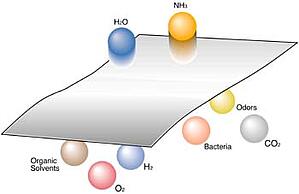
Permeation barriers for electronic devices are essential to assure their ongoing performance through a wide range of operational environments. Polymer flexible conformal coatings provide good barrier protection, protecting device substrates from unwanted incursion by solid contaminants, chemicals, gaseous permeation and liquid water or vaporous forms of moisture. Permeability reduction improves with enhanced coating adhesion, minimizing the surface's
Disrupting the thermo-mechanical properties of printed circuit boards (PCBs) and related electrical assemblies, excess moisture caused by uncontrolled WVTR leads to:
 Conformal protection controls moisture-originated performance issues; success-level depends on the film-material used. Parylene (XY) generates reliable surface adhesion and barrier protection, sufficient to withstand permeation by most substances under a wide range of operating circumstances.
Parylene chemical vapor deposition (CVD) generates the thinnest available conformal coatings for most uses, with excellent substrate coverage. XY typically provides effective barrier protection at film thicknesses ranging from 0.013 – 0.051 mm. (0.0005 to 0.002 in.), but coatings are controllable to less than a single micron (1 μm/1,000 nms). The exceptional uniformity of pinhole-free XY prevents leakage; vaporous coatings seep deep into substrate surfaces during application, providing additional moisture protection.
The impact of CVD processes on the surface morphology and molecular structure of both deposited parylene and the substrate influence the coating’s conformal barrier properties. Operating in a vacuum, CVD transforms solid parylene dimer into a gas, which penetrates within substrate surfaces as well as forming the exterior encapsulating film. The process effectively generates an internal, as well as external protective layer, maximizing XY’s barrier protection. CVD creates a conformal film unmatched by liquid processes of such coating materials as acrylic, epoxy, silicone and urethane.
Relevant CVD process parameters include the time duration of the deposition process. its growth rate, and both pyrolysis and sublimation temperatures. Appropriate control of these factors develops measured growth of barrier layer thickness, across a span of tens of nanometers to the 20+ μm range, generating reliable, longer-term film barrier stability. The coating’s electrical properties are also significantly improved by CVD-processing; this is particularly the case for pyrolysis temperature modification. Optimizing CVD process control improves film reproducibly and compatibility for a wider range of application domains.
Parylene coatings are uniform at controllable, pinhole-free thickness. XY remains adherent and intact, preserving dielectric/insulation properties, at thicknesses greater than 0.5µm., completely penetrating spaces narrow as 0.01mm. Unlike liquid coatings, parylene’s CVD penetration coats all aspects of an assembly, regardless of surface topography, engendering a truly conformal barrier coating, both above and below component surface.
Parylene resists chemicals, corrosives, moisture and solvents, with minimal thermal expansion, covering virtually any board topography, while ensuring PCB/assembly function/performance through most operating conditions. In addition, chemically inert parylene has outstanding chemical resistance -- sustaining PCB function in harsh environments, characterized by atmospheric pollutants and aggressive solutions – better than liquid coatings. Heat resistance is also very dependable; XY’s dielectric properties are high, well protected by its ongoing barrier strength.
Basic Dielectrics and Conformal Coatings
A dielectric substance is an electrical insulator with the additional property of transmitting electricity without conduction. Dielectric mediums are efficient supporters of electrostatic fields that also dissipate thermal energy at a minimal rate; thus, they have the potential to store energy. The parameter encompassed by a substance's dielectric constant is a common source of comparison in the design of printed-circuit-boards (PCBs) and similar higher-speed electrical components.
The lower the dielectric constant, the less the extent to which a material concentrates electric flux, Composed of weakly bonded molecules, lower dielectric-constant substances such as parylene conformal coatings produce a reliable barrier between a substrate and its environment. Polarized by electrical charges, they resist electrical conduction and therefore can be effectively used to coat the high-speed electrical components common to IT, biomedical and communications' media.
Essential Dielectric Properties of the Parylene
Parylene conformal coatings are known for their documented dielectric properties. Highly corrosion resistant, dense and pinhole free, they provide a completely homogeneous coating surface. Dielectric properties differ according to parylene type. For instance, the average in-plane and out-of-plane dielectric constant for parylene N is 2.65, while parylene C is 2.95. Other parylene types range between 2.25 - 3.15. Table 1 provides a further dielectric comparison of major commercially viable types of parylene.
Dielectrical properties of Parylene N and C
Dielectrical Strength, V/ml
Parylene N: 7,000
Parylene C: 5,600
Dielectric Constant
Parylene N: 2.65 @ 60Hz
Parylene C: 3.15 @ 60Hz
Parylene N: 2.65 @ 1KHz
Parylene C: 3.10 @ 1KHz
Parylene N: 2.65 @ 1MHz
Parylene C: 2.95 @ 1MHz
Dissipation Factor
Parylene N: 0.0002 @ 60Hz
Parylene C: 0.020 @ 60Hz
Parylene N: 0.0002 @ 1KHz
Parylene C: 0.019 @ 1KHz
Parylene N: 0.0006 @ 1MHz
Parylene C: 0.013 @ 1MHz
Parylene's Dielectrical Performance Relative to Other Conformal Coatings
In comparison to competing types of conformal coating, parylene's lower dielectric constants reflect its capacity to withstand intense electrical fields. One of its advantages as a surface coating is a considerably lesser tendency not to devolve when subjected to significant electrical activity. Competing coatings have higher dielectric constants (Epoxy, 3.3 - 4.6. Polyurethane, 3.8 - 4.4, Silicone, 3.1 - 4.2), and a lower non-conductive capacity. Their dielectrical strengths are also lower (Epoxy, 2200. Polyurethane, 3500, Silicone, 2000), indicative of the diminished ability to provide dielectric protection compared to the parylenes.
Substances with higher dielectrical readings break down much more readily during prolonged contact with intense electrical activity. On the odd chance that parylene does suddenly begin to conduct current and is subjected to a dielectric breakdown, the condition is temporary, subsiding with removal of the excessive electric field. At that point, parylene reverts to its normal, non-conductive dielectric state and does not sustain permanent damage.
Advanced Applications Aided by Parylene's Dielectrical Properties
Parylene's dielectrical capacities have extended the utility of existing products and aided in the development of new ones. Among current applications are:
Conclusion
When tested for dielectric withstanding, at 1500 Vrms/0 Hz, using method 301 in accordance with Mil-Std-202, parylene's electrical resistance measured 10% or less of the maximum allowed requirement. These low scores further represent the superior dielectric qualities of parylene conformal coatings. They do not conduct electricity but nevertheless sustain an electric field, permitting the safe passage of electrostatic lines of force through protected components.