
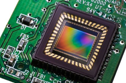
Microelectromechanical systems (MEMS) consist of technologies whose operative components range between 1-100 micrometers in size.
Choosing the Best Protection
Microelectromechanical systems (MEMS) consist of technologies whose operative components range between 1-100 micrometers in size. The micronization of MEMS devices and structures (their mechanical and electro-mechanical elements) is a consequence of developments in modified semiconductor fabrication technologies originally used for electronics.
 The basic defining characteristic of MEMS is mechanical functionality, regardless of components ability to move physically within their product casing. However, this definition can be deceiving. Although some MEMS devices have no moving parts, many are complex electromechanical systems, with multiple moving elements managed by integrated microelectronics. Combining microelectronics, microactuators and microsensors with related technologies, thus integrating their functions onto a single microchip, is expected to be one of the future's most significant technological breakthroughs.
Coating MEMS
MEMS products are frequently used in areas of high functional activity and stress. Prevailing environmental conditions can compel protection from exposure to temperature extremes, abrasive liquids, or similar circumstances that can generate product degradation or malfunction. Micronized components also frequently suffer from stiction -- friction that interferes with stationary surfaces being set in motion during operation.
Under these conditions, it is necessary to protect components by depositing exceptionally thin films of covering material onto substrates during MEMS processing. Depending on the MEMS component and its uses, these coating layers may need to be as thin as five nanometers to effectively minimize stiction, while providing insulation and otherwise securing components' functions. Coatings exceeding 100 micrometers interfere with components' performance, rendering them ineffective for MEMS purposes.
Conventional liquid-phased, monolayer coating processes, such as spraying and dipping, have proven less useful for MEMS purposes. Vapor deposition processes are more effective for MEMS because they completely eliminate the wet deposition methods necessary for such coating materials as epoxy, silicone, or urethane. Thus, many conformal substances using these methods -- acrylic, epoxy, silicon, urethane -- have fewer applications for MEMS, unless they can be adapted to vapor-phased anti-stiction techniques, which are superior.
Mechanical deposition processes for MEMS include:
Physical Vapor Deposition (PVD): Of value for metal deposition, PVD coatings such as diamond-like carbon (DLC) generate low levels of stiction and high micro-hardness. However, film quality is inferior to chemical vapor deposition (CVD), with lower substrate adherence, higher resistivity, more defects and blemishes along surfaces. Limited and specialized application suggested.
Casting: Coating materials are dissolved in a solvent and applied to the substrate in liquid form by spraying or spinning. A thin film of coating material – organic photoresists, polymides, epoxy -- remains on the substrate following solvent evaporation, in the range of tens of micrometers. Limited applications for polymers, metal and glass.
Chemical deposition processes for MEMS include:
Thermal Oxidation: This very very basic deposition technology is effective only for materials that can be oxidized. Temperature levels of 800°C -1100°C accelerate the coating process. Diffusion of oxygen into the surface can form silicon dioxide on a silicon substrate; substrate penetration improves electrical insulation. Unfortunately, coatings thicker than ~100 nanometers can generate additional surface films that restrict use for MEMS applications.
Electrodeposition: Limited to electrically-conductive materials, substrate surfaces may require a previously-applied electrically-conductive coating before deposition can be enacted. In these cases, electrodeposition generates reliable conformal coatings for metals such as copper, gold and nickel, at thicknesses of ~1µm to >100µm. However, film thickness and uniformity are difficult to control; limited application suggested.
Chemical vapor deposition (CVD): The most reliable MEMS coating technology, higher CVD process temperatures yield a coating surface of better quality, with fewer defects. Parylene stands out in this respect. Its conformal coatings are effective at thicknesses as slight as 0.1 microns, making them exceptionally adaptable for MEMS uses. Further beneficial qualities of CVD-deposited parylene include:
Parylene's CVD processes best assure precise MEMS-coating thicknesses, where even an additional micrometer of coating can generate component dysfunction or failure.
Conclusion
Semiconductor-made micro-mechanisms, MEMS demonstrate virtually unlimited potential for a multiplicity of rapidly evolving products: aerospace/automotive systems, consumer electronics, IT, telecommunications, and medically biocompatible/implantable materials' uses, as well as ruggedized military applications of all types. Capacities for further product development and sophistication of MEMS are expected to proliferate in the future.
Because of their size and need to function through a diversity of frequently difficult conditions, MEMS components require exceptional protection. CVD-applied coatings provide the most durable and flexible coatings, able to withstand an extreme range of problematic operating conditions. Of available coating materials, parylene is the most widely used and the most reliable.
How it Protects
Parylene is proving to be an ideal material for sealing, insulating, and protecting electronic modules, devices, and circuit boards. It’s easy to apply, goes down in uniform layers, and stands up to many environmental hazards. These same properties also make Parylene an excellent choice for manufacturing micro-electromechanical systems (MEMS) – sensors, actuators, and structures forged from silicon using industry standard semiconductor-processing techniques. In fact, Parylene is helping MEMS designers overcome some of their toughest challenges, clearing the way for new features and functions and a fresh growth spurt for MEMS applications.
From the time silicon was first used to form mechanical structures and devices, designers have struggled with space constraints on both ends of the dimensional spectrum. MEMS devices – accelerometers, gyroscopes, and flow sensors, for example – typically contain many complex moving parts as well as signal processing and interface circuits, and all these elements must fit comfortably in packages scaled to size of tiny silicon chips. At the same time, every nook and cranny in the labyrinth of silicon micro-machinery must be accessible to fluids and light fields employed in the many processing steps. Parylene excels under such circumstances because it’s applied in a gaseous or vapor state under vacuum. The vapor deposition process uniformly coats even the most inaccessible surfaces, penetrating spaces as narrow as 0.01 mm. It also covers sharp edges, points, and exposed internal surfaces, resulting in a thin conformal layer that’s free of pinholes and impermeable to anything larger than 1.4 nanometers (nm).
Another challenge MEMS designers face stems from thermal and mechanical stresses imposed by the presence of sealing materials as well as the processes by which they’re typically applied. Thick heavy coatings, for example, can reduce the sensitivity and dynamic range of motion sensors and actuators. The effects of high processing temperatures, on the other hand, are potentially worse and may even be catastrophic. Parylene circumvents both problems. For one, it’s applied at room temperature and it doesn’t require curing like many other coating materials. It also minimizes mechanical stresses and loads because it can be applied at a precisely controlled thickness. Parylene layers form on substrates literally one molecule at a time, resulting in uniform films that can be anywhere from a few angstroms to several microns thick.
Even at a thickness of just 0.5 microns (µm), Parylene achieves a near impenetrable defense for the surfaces and structures it protects. Not only does it provide a pinhole-free moisture and chemical barrier, but also a biological barrier. What’s more, components sealed with Parylene are unaffected by solvents, including gasoline and acetone, and can easily pass a 100hr salt-spray test. Besides being chemically and biologically inert, Parylene offers outstanding wear and dry-film lubricity properties with a static coefficient of friction near that of Teflon – as low as 0.25 to 0.30. It’s also stable over a wide temperature range (-200‘C to +200‘C) and is extremely rugged, having high tensile and yield strength in the range of 50 to 70 MPa.
Parylene’s electrical and optical properties are also well suited for MEMS applications. Parylene is a good electrical insulator with high dielectric strength and high bulk and surface resistance. It also has negligible capacitive effect thanks to its low dielectric constant. This mitigates parasitic losses that would otherwise occur at high frequencies. As for its optical properties, Parylene is relatively transparent and can be used to coat LEDs, light sensors, mirrors, and lenses. It also withstands UV radiation and protects optical components from UV-induced damage. Parylene can be applied to most vacuum-stable materials, including optical plastics, metals, quartz, and semiconductors.
Advantages of Parylene
In the past decade, the use of Parylene as a structural material in microelectromechanical systems (MEMS) devices has attracted significant attention. Parylene C, known for its biocompatibility, is widely used in implantable medical devices. Parylene C is also compatible with MEMS microfabrication processes.
What are MEMS?
Microelectromechanical systems (MEMS) is the technology of very small devices; it merges at the nano-scale into nanoelectromechanical systems (NEMS) and nanotechnology. MEMS are made up of components between 1 to 100 micrometres in size (i.e. 0.001 to 0.1 mm), and MEMS devices generally range in size from 20 micrometres (20 millionths of a metre) to a millimetre (i.e. 0.02 to 1.0 mm). They usually consist of a central unit that processes data (the microprocessor) and several components that interact with the outside such as microsensors.
What is Parylene?
Parylene is a polymer applied through a deposition process. Parylene coatings are completely conformal, have a uniform thickness and are pinhole free. Parylene is chemically and biologically inert and stable and make excellent barrier material. Parylene has excellent electrical properties: low dielectric constant and loss with good high-frequency properties; good dielectric strength; and high bulk and surface resistance.
Parylene and Technology
Parylene has an easy coating process, controllable conformal coating thickness, and is highly compatible with the plasma etching process. As a result of this, parylene has been easily integrated with the fast growing MEMs technology. An example of current usage would be neuron cages, which are manufactured using a multiple parylene layer etching process. Another current use is parylene enabled retinal ocular implants.
Sources:
Parylene Technology for Neural Probes Applications. Changlin Pang. California Institute of Technology. Pasadena, California. 2008.
A Parylene MEMS Electrothermal Valve. Po-Ying Li et al. J Microelectromech Syst. 2009 December; 18(6): 1184–1197. doi: 10.1109/JMEMS.2009.2031689.
How it Protects
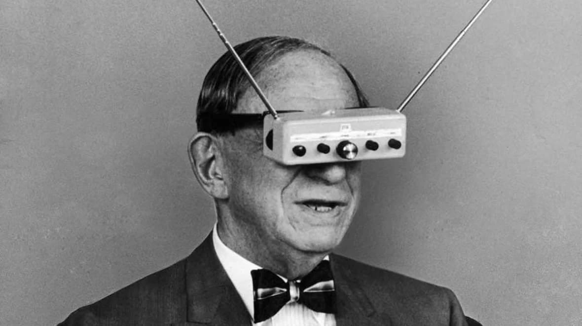
Wearable devices have become familiar, ever more an integral component of everyday life, with expanded uses for many conventional activities. Advanced med-tech -- ranging in format from external exercise monitors to implanted cardiac pumps, defibrillators and deep-brain sensors –- represent only a fraction of wearable medical devices currently applied for healthcare and treatment. Smartphones and watches can be found everywhere; smart fabrics are used with increasing frequency for clothing and textiles. Wearables reflect the expanding scope of the Internet of Things in most areas of human endeavor.
As use of wearables grows, manufacturers try to determine the optimal mix of form, function and technology that will encourage further consumer/ professional application of the devices. In healthcare, wearables provide a range of status indicators (heart rate, physical activity levels, etc.) that monitor individual’s engagement of healthful (or unhealthy) activities. In addition to focusing on improving their functional technology, battery life and consumer fashion, the need to safeguard wearables performance is a prominent concern. All wearable devices are informed by technologies that need conformal protection for and from their functional environments. Parylene films are the most appropriate choice for protection in just about every case.
Parylene as a Safeguard of Wearable Functionality
Wearables of all kinds possess sensors; these include items like artificial magnetic conductors (AMCs) and light-emitting diodes (LEDs), that support wearable functionality while recording their own and their wearers’ activities. This is particularly the case for microelectronicmechanical (MEMS) and nanotech (NT) sensors, which can require both
Parylene conformally coats even the smallest and most complicated item with resilient, ultra-thin film, generating functional superiority for safeguarding MEMS/NT.
Current applications of parylene as a conformal coating for components of wearable devices include:
While parylene’s effective, thin-coat dielectric properties
In this regard, masking prior to parylene chemical vapor deposition (CVD) prevents its deposit on wearable sensors and related components, securing efficient operation, while retaining the protection of conformal coating for the remainder of the unit.
Parylene’s collective properties support the real-world performance expectations inherent in wearables. They generate a truly conformal film that resists water and body sweat, as well chemicals, corrosives and solvents, protecting the device’s function and performance whether worn on the body or implanted internally. Parylene performs reliably at normal body temperature, withstanding as well a temperature range between -200° C through 80° C, with no appreciable operational degradation.
Biocompatible, micro-thin parylene is exceptionally light weight, assuring non-irritating performance, whether worn against the skin or implanted; dry- film lubricity further adds to comfortable functionality. The parylene coating prevents gasses from entering the wearable, resisting physical abrasion and impact as well, a matter of concern, since wearables are often worn on the body and can be exposed to real-world environmental conditions; these include but are not confined to persistent bodily excretions, direct sunlight/UV rays, variable electrical signals, acidic/salt solutions/sprays, and motion/vibration.
Conclusion
The market for wearable sensory and related technologies for both consumer products and in healthcare is expected to grow significantly through the mid-future. Although much needs to be done to improve wearable functionality, parylene conformal protection should evolve with continued development of both wearable and parylene technologies. For instance, innovations in wearable medical technology will further explore the intersection between physical and digital worlds, as an increasingly standard provision of patient care; a similar direction is anticipated for the future’s wearable consumer products.
All wearable devices are only as functional as the protection they receive. Effective at thicknesses measured in microns, parylene provides optimal conformal security for wearables of all kinds. In addition to exceptional water resistance, parylene conformal films also secure wearable devices against sweat, EMF/RF signals, humidity, caustic solutions emanating from both inside and outside the body, and chemical exposure. No other conformal coating can provide this range of safeguards for wearables.
If you're looking for parylene coating services for MEMs, contact Diamond-MT today. Get started by calling us at 814-535-3505 or completing a quote request.