
Whether the application is a medical device, a printed circuit board (PCB), or a light-emitting diode (LED), a parylene conformal coating is typically applied to protect the product. Sometimes, however, the product actually has to be protected from the parylene conformal coating—or at least parts of it do.
Materials and Methods
Parylene deposition takes place at the molecular level. Applied at room temperature through CVD processing, the typical thickness of parylene conformal film is in the microns-range.
Advantages of parylene coatings include:
Despite its benefits, parylene has several major disadvantages. Among these are:
A further disadvantage is the need for costly, time-consuming masking of selected assembly components. The parylene masking process is necessary to protect designated areas of an assembly that could impede performance if coated.
Masking
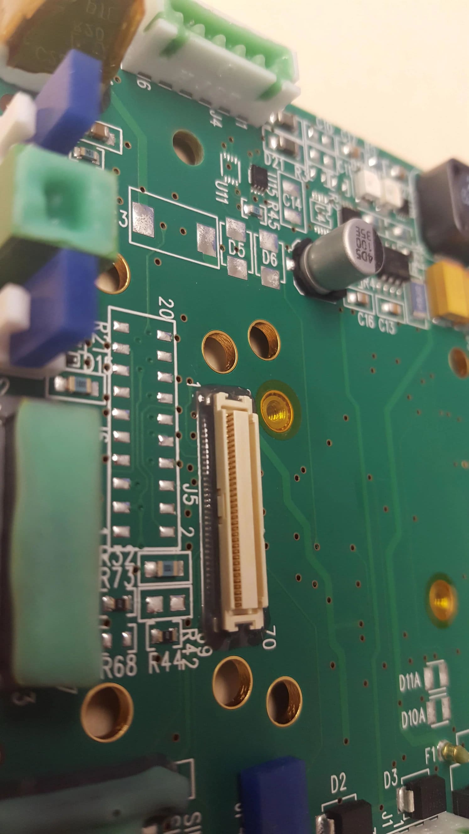
Masking assures selected assembly components are NOT covered by the applied parylene film, which would inhibit their functionality. Integral to surface preparation, the masking process protects designated assembly components from the encapsulating effects of the parylene itself, which would suspend their operational capacities.
For instance, parylene’s excellent dielectric properties simultaneously disable a PCB's contacts, rendering the unit inoperable, even as the substrate is protected from electrical interference. Masking contacts resolves this issue, coating only those PCB parts that aren’t distressed by conformal protection. Components retain their capacity to accept an electrical charge and/or move as designed.
Masking Materials
Masking requires different materials such as peel-able masking dots, tapes/contact pads, boots and either non-ammoniated or water-soluble liquid latex. It is important to recognize:
Parylene masking dots and tapes generally use polyester or polyimide backings. In the vast majority of cases (90%+), properties like conformability and cost-effectiveness are as necessary to the masking process as strength and stability.
Essentially, masking dots are small stickers fastened over the contact before coating is initiated.
For masking tapes and contact pads, there are two widely used solutions:
Unless a popular part like a Molex connector is being used, masking boots are typically custom-made, specific to the physical configuration of the component to-be-covered. Recyclable, boots’ capacity for repeat processing is a labor-saving initiative that also generates considerable cost-effectiveness during re-use, recouping the initial investment in short order.
Masking Methods
Generally, the most labor intensive part of the coating process, masking is done in accordance with the customer’s drawings and requests for coating keep-out areas. Because CVD causes parylene molecules:
Basic to the process is accurately identifying those sections of the assembly NOT to be covered during CVD. A general methodological outline includes these steps:
These processes are exceptionally labor-intensive and can be costly. Nevertheless, they are essential to parylene film administration. Touching up the periphery of the masked region with a small quantity of urethane after removing the masked materials lessens the threat of tears.
For most applications, use of conventional masking materials and techniques obstructs parylene deposition on designated PCB keep-out regions. However, masking for MEMS/nano medical devices is more challenging. Laser ablation provides better options for these more difficult applications, enhancing adaptability to assembly’s alternate geometries, while providing greater precision during mask application.
Masked regions are protected from coating, assuring they function as designed to generate appropriate assembly performance. Masking materials must thoroughly shelter the keep-out regions, without gaps, crevices or similar surface breaches, to provide reliable connector function after coating. Effective masking of each PCB connector demands concerted operator attention, to appropriately seal it from contact with gaseous parylene molecules during CVD. Masking preserves an assembly’s operational integrity and performance.
A Final Word
Integral to a complete masking solution for PCB conformal coating, masking boots protect selected components located in keep-out areas, to assure they remain operative after coating. Reusable boots provide a strong, cost-effective alternative to such materials as masking tape and dots. Masking boots can be custom configured into all forms, shapes and sizes to protect an extreme variety of assembly components from coverage for most conformal coating application techniques.
Reasons for Masking Parylene Coating
Whether the application is a medical device, a printed circuit board (PCB), or a light-emitting diode (LED), a parylene conformal coating is typically applied to protect the product. Sometimes, however, the product actually has to be protected from the parylene conformal coating—or at least parts of it do.
That's where parylene masking comes in. The parylene masking process serves to protect designated areas of an assembly that could negatively impact performance if coated. And because masking parylene coating preserves the functionality, integrity, and performance of an assembly, it is among the most crucial steps in the parylene coating process.
Reasons for Masking Parylene Coating
Some of parylene's key properties can be both desirable and detrimental to an assembly, depending on where the conformal coating is applied. For example, parylene is an excellent dielectric. As a result, a parylene-coated PCB will be protected from electrical interference. If the PCB's contacts are coated, however, the board won't work. Parylene masking solves this conundrum by allowing the board to be selectively coated in order to reap the benefits of parylene without rendering the PCB inoperable.
Masking parylene coating is also performed when an area of a device or component has a moving part. If these parts are coated, the parylene coating could be damaged by the motion of the part. Masking these parts serves to protect the integrity of the parylene coating.
Parylene Masking Process
Although masking parylene coating is among the most time-consuming and labor-intensive steps in the parylene conformal coating process, it also among the most important. Improper or poor parylene masking, after all, can compromise the coating or cause failure of the finished part.
When working with a contract coatings company, the first step in the parylene masking process is to generate drawings that clearly identify the areas of the product that should not be coated during parylene deposition. Once the product has been delivered, the mask has been designed, and the substrate has been cleaned in preparation for parylene deposition, masking materials are applied to the areas that must remain uncoated.
Once the product is masked, it is placed into the vacuum chamber for parylene deposition. During this stage of the process, parylene vapor envelops the entire product, covering any surface of the substrate that is exposed to air. On the masked areas, however, the parylene is deposited on the masking materials instead of on the actual substrate. The masking material is then removed when the product is dry, taking the parylene coating with it.
Alternatives to Masking Parylene Coating
While parylene masking and mask removal are time-consuming and exacting processes, the alternative approach is to coat the entire product and then selectively remove the parylene coating from the specified "coating-free" areas. And while this approach can yield success, it poses its own challenges.
Parylene removal can be accomplished through thermal, mechanical, and abrasion methods. Thermal and mechanical methods, however, carry a high risk of damaging the substrate. Abrasion—which uses a technique that is similar to sandblasting, albeit on a near-microscopic scale—can produce accurate and cost-effective results. On the other hand, it is still more labor intensive than applying a mask and selectively coating the substrate.
Depositing and masking parylene conformal coating are complicated processes with many variables and challenges. But when performed correctly, parylene coating offers a degree of protection and performance that few other types of conformal coatings can match.
Masking and Parylene Deposition
Parylene deposition is a complicated process that needs to be effectively monitored to ensure its superior levels of protection and performance. However, inappropriately applied parylene can sometimes have an adverse effect on the functionality, integrity, and performance of an assembly or component. Masking selected regions of a substrate is an essential part of the parylene coating process.
Examples of Potential Product Failure
Parylene conformal coating does an incomparable job of protecting product substrates from harsh, unpredictable operating environments of all kinds. However, while most of parylene's key properties -- barrier strength, dielectric, flexibility, lubricity, etc. -- are exceptionally useful to a part or assembly, much depends on where the conformal coating is applied. Because parylene coatings are so effective, covering inappropriate areas of a component can have a negative impact on its overall performance, defeating the basic purpose for parylene application.
In this respect:
In the case of printed circuit boards (PCBs) and similar electrical devices, parylene's superior dielectric qualities are detrimental, precisely because they conduct electricity poorly. Masking ensures electrical contact points are uncovered and operable, allowing them to fulfill their function. Parylene covering of moving parts can not only retard their motion, and thus impede their functionality, but will also damage the coating itself, diminishing the overall integrity of the parylene coating throughout the component.
Masking provides the best solution yet devised for these circumstances, which are common to many of parylene's product uses. By ensuring the circuit board, contact point or moving part remains uncoated, while the remainder of the product is effectively and conformally covered, masking resolves these issues; the many advantages of parylene are accessed, without suppressing the product's ability to function as designed.
The Parylene Masking Process
While very necessary, the parylene masking process is also costly and time-consuming. Several steps encompass the masking process and ensure proper implementation:
Do It Right
You'll want to make sure the masking process is properly implemented. Not only is this necessary to preserve the product's integrity, guaranteeing it works as designed, but also because of parylene's superiority as a conformal coating. Very simply, once bonded to a substrate, parylene is exceptionally difficult to remove. If masking is unsuccessful, further time and expense will be wasted removing parylene from the product's sensitive regions, potentially damaging the conformal coating throughout the product. The expensive, time-consuming processes of both masking and coating will have to be repeated to assure product functionality and protection.
Pre-coating Essentials
Poor parylene adhesion negates many of the coating’s most-valued functional properties, including dielectric strength, and resistance to the effects of chemicals, corrosive agents, and moisture. Surface treatments that amplify the interface adhesion between the deposited parylene and the coated substrate are therefore highly desirable. These treatments entail depositing parylene on a clean hydrophobic surface before its chemical vapor deposition (CVD) process is enacted.
Parylene is applied to substrates at ambient temperatures within a specialized vacuum, conducted at pressures of around 0.1 torr. To assure complete impingement of the parylene monomer, uniformly encapsulating the substrate, provision of appropriate surface support prior to CVD limits subsequent factors of peeling force, soaking undercut rate, and vertical attack bubble density (VABD). that can lead to lack of coating adhesion and delamination.
A truly conformal coating, parylene provides superior, uniform barrier protection on almost any surface geometry or topography. However, any contaminants present on a substrate surface prior to CVD will inevitably have a negative impact on parylene adhesion. Chemicals, dust, oils, organic compounds, process residue, wax – contaminants of any kind – need to be thoroughly removed, leaving the substrate surface entirely devoid of their presence; if unattended, issues such as mechanical stress can develop. Contamination generated by dirty surfaces can stimulate coating delamination and severe degradation of affected operating systems, as the parylene coating begins to disengage from the surface.
Cleanliness Inspection and Testing
Thorough surface inspection is the first step to delivering a substrate surface suitable to parylene adherence. Identifying contaminants significantly lowers the risk of incomplete surface cleansing, while informing selection of task-appropriate materials and methods.
Costly cleaning and rework issues can emerge if thorough surface-inspection is overlooked at any stage during the production/coating process. Poor inspection fails to detect and identify contaminants, leading to delamination, exposed surfaces and component dysfunction. In such cases, it is not uncommon for leakage of non-organic, electrically-conductive sediments beneath the parylene to interfere with and ultimately wreck the performance of electrical components.
Useful surface inspection techniques for organic contaminants include Gas Chromatography (GC) and Fourier Transform Infrared Spectroscopy (FTIR). Sometimes used in conjunction with mass spectroscopy, GC splits unidentified organic chemical mixtures into their distinct components, specifying their discrete properties. FTIR identifies specific organic contaminants by comparing evidence from spectrum analysis to those of known substances; contaminants such as silicon oils and mold-release agents are identified with FTIR. Valuable for determining the presence of inorganic contaminants like chloride, fluoride, potassium, or sodium, Ionic Exchange Chromatography (IOC) uses electrical-charges to separate the compounds’ ions and polar molecules.
Parylene Surface Cleaning Agents
A variety of nonhazardous cleaning agents can be effectively applied to substrates, according to their precise identification. Regular detergent cleaning is suggested for soluble contaminants. Less soluble contaminants require use of biodegradable, multi-faceted, solvent-strength solutions like deionized water, isopropyl, and methyl ethyl.
Cleansing methods are also dependent on the composition of both the identified contaminants and surface materials, to achieve satisfactory levels of substrate neutralization. Solvent immersion, surface-spraying, substrate-tumbling, or vapor-degreasing are primary disinfectant procedures. However, the substrate surface may also require manual, hand-cleaning, or application of batch, inline, or ultrasonic methods.
Masking
Integral to surface preparation, the masking process is implemented to assure designated components of a PCB or similar electrical assembly are protected from the effects of the parylene itself, which can interfere with expected functionality. Some of parylene's key properties can be both desirable and detrimental to an assembly, if applied to the wrong areas. For instance, parylene’s excellent dielectric properties simultaneously disable a PCB's contacts, rendering it inoperable, even as they safeguard the substrate surface from electrical interference.
Masking the contacts resolves this issue, coating only those PCB-parts that won’t be negatively impacted by conformal protection. In this way masking preserves an assembly’s operational integrity and performance. This critical pre-phase of the parylene coating process can be exceptionally labor-intensive. Considerable operator attention to the task is necessary to ensure effective masking of each connector, sealing it from penetration by gaseous parylene molecules during deposition. All tape, or other covering materials, must thoroughly shelter the keep-out regions, without gaps, crevices or other openings, to ensure connector function is retained after coating.
A-174 Silane
A-174 silane adhesion promoter chemically bonds with the substrate surface to stimulate resolute parylene adhesion. Manual-spray, soaking, or vapor-phase processing methods are used to apply A-174 to the substrate after the masking-operation, forming a chemical bond with the surface. Substrates responding well to treatment with A-174 silane prior to implementation of parylene coating processes include those made of elastomer, glass, metal, paper and plastic.
A-174’s molecules form a unique chemical bond with the substrate surface, sufficient to improve parylene’s mechanical adhesion. However, not all substrate materials benefit from A-174. In its place:
Researchers continue to seek additional cleansing/adherence agents to improve parylene's conformal utility for these purposes.
The diversity of adhesion promotion methods requires a similarly diverse list of raw materials and techniques. Surface treatments prior to CVD begin with cleanliness-testing and cleaning to remove surface contaminants, followed by masking of connectors and electrical components. Materials such as glass, metal, paper and plastic benefit from application of A-174 silane adhesion promoter for necessary, pre-CVD surface modification. Establishing best-adhesion practices and strict adherence-standards is critical to maintaining quality conformal coatings and minimizing delamination.
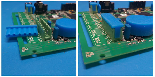
Styles of Masking Boots
With proper equipment and professional expertise, liquid conformal coatings and vapor-applied parylene readily provide printed circuit boards (PCBs) and similar electronics a durable overlay of protective, insulative film; parylene’s CVD processes ensure the coating actually penetrates the substrate surface, generating further device security.
However, the very insulative properties that help conformal coatings safeguard PCBs will negate the performance of such critical electrical components as capacitors, connectors, diodes, resistors, or transistors, blocking their ability to transmit or receive electrical signals. Protecting PCB components> from the encapsulating properties of conformal materials, which would suspend their operational capabilities is imperative. These keep-out areas require masking prior to initiating the coating process, to assure designated PCB components are NOT covered.
Also called caps or plugs, custom reusable boots surpass masking tapes or dots for assignments demanding an explicit volume of repeat-masking. Efficiently covering PCB’s electronic components, masking boots ensure reliable performance, preventing coating seepage onto and within keep-out regions. In addition, boots don’t leak as frequently as tapes or dots, eliminating the need for masking (and coating) re-work, adding significantly to their return on investment (RoI). They are also better adapted to accommodating the masking needs of a wider range of component shapes and sizes.
Other masking solutions often necessitate costly, labor-intensive and time-consuming processes, limiting RoI while delaying project completion. Fastening over often large areas of the PCB, boots provide a labor-saving alternative for:
Resulting reduction in both masking and demasking time/labor shaves as much as 75% off operating costs. Moreover, reusable boots do not require constant replacement (repurchase); some can be used 200(+) times before replacement is necessary! The initial investment constructing custom-made boots is rapidly recovered through their continual reuse, rather than the ongoing replacement required for tapes and dots.
Different Styles of Masking Boots:
Masking materials come in various forms; among the most prominent are
Effective masking requires coordinating masking types and materials with the specific masking project. Tapes/dots/contact pads are frequently the choice for many projects where less expansive surface areas require coverage; cover/plugs are easy to use for specified masking purposes. Masking boots are recommended for larger projects, especially those characterized by irregular board topographies.
Designed to flexibly cover larger PCB components, recyclable masking boots readily accommodate projects requiring repeat masking of high-volume production. The most common boot materials are silicone rubber and similar low- hardness elastomers, which offer:
Electrostatic discharge (ESD) resistant boots are always available, generally at higher cost. Custom-boot sizes and colors are adaptable, dependent on coating project specifications; boots’ material composition varies to encompass:
Once these factors have been determined, criteria for determining the assignment’s proper boot configuration are better defined Masking boots have two basic format styles: A and C type Cups:
While boots are not recommended for dip applications, they are very efficient for spray treatments and other liquid-application procedures; production turn-around is fast and reliable. The same is true for most parylene CVD processes. However, A-type molex boots applied for spray-shielding purposes may begin to deteriorate over time, causing coating-seepage into the component. Boot replacement is then necessary. These factors largely determine assignment boot type, whether standard or customized.
Reusable boots provide a strong, cost-effective alternative to masking tape or dots. Depending on your conformal coating needs, Diamond-MT offers clients a variety of standard and custom boot solutions. We have a wide range of standard boots in stock, to be matched to your project specifications. Our design services can also develop a custom masking solution to accommodate your specialized PCB components.